Dec 2015- Feb 2016: Research work as a postdoctoral researcher at RIEC, Tohoku University, Japan
SiC power device evaluation using scanning non-linear dielectric microscopy (SNDM).
Silicon Carbide (SiC) is a wide band-gap semiconductor material that can sustain high voltages (~ 10 kV) and high temperatures. Similar to Si, SiC also has SiO2 as its native oxide layer. These properties enable it to be a promising candidate for power electronics. SiC-MOSFETs are now commercially available but they have serious problems (e. g. low channel electron mobility and threshold voltage variation) whose origin is thought to be the insufficient quality of SiO2/SiC interface. In order to improve the interface quality, microscopic details of the interface need to be revealed.We investigated SiO2/SiC interface using SNDM, which is a kind of scanning probe microscopy (SPM) that measures capacitance (Cs) response to the applied voltage between metal-coated tip and sample. The resulting image of SNDM measurement is 2D mapping of ∂Cs/∂V which has strong correlation with carrier distribution. Following is a schematic explaining the principle of SNDM.

Upon investigating various SiC samples (Si-face, C-face, a-face), we obtained very strong correlations between SNDM image and interface-state density Dit as well as channel electron mobility μFE.The unique feature of this technique lies in the fact that it can detect extremely small capacitance variation between the tip and sample.
This technique can be widely applicable for evaluation and development of next generation high performance electronic devices, for example, flash memory, GaN power devices, solar cells and ultrahigh density ferroelectric data storage, etc..
2009- 2014: Research work as a postdoctoral researcher at NIMS, Japan
1. Fundamental research on atomic switches to reveal the operating mechanism and their characteristics using scanning probe microscopy.
Atomic switch is an electrochemically controlled nanoscale resistive switching device that switches between a low-resistance on-state to a high-resistance off-state due to the formation and annihilation of metal atoms bridge between two electrodes. Switching properties of Ag2S, Cu2S, and RbAg4I5based gap-type atomic switches were studied using a scanning tunneling microscope. The experiments included measuring the switching time depending on bias, temperature and initial off-resistance conditions. The rate-limiting steps of switching processes were revealed. An ultimate lateral, mass and charge resolution during electrochemical Ag phase formation at the surface of RbAg4I5 was also achieved (Nature Materials 2012, 11, 530-535). Following are some results of this work:

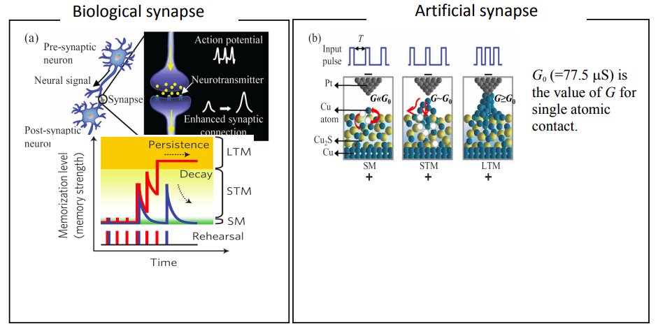
2. Demonstration of artificial synapse operation,using the concept of atomic switch, which will contribute to the development of neural computing systems.
Cu2S gap-type atomic switch, referred to as a Cu2S artificial ( inorganic) synapse, emulates the synaptic plasticity underlying long-term memory (LTM), short-term memory (STM) and sensory memory (SM) formations in the human brain. The change in conductance (G) of the Cu2S atomic switch is considered analogous to the change in strength of a biological synaptic connection known as the synaptic plasticity. Following is the schematic representation of this work (Adv. Funct. Mater. 2012, 22, 3606)

3. Two-terminal resistive switching memory devices based on the concept of atomic switch.
Cu/Ta2O5/Pt resistive memory device was studied for position detection and observation of a conducting filament (CF) hidden under a top electrode using conductive atomic force microscope. The accomplishments of this work are presented below (Nanotechnology 2015, 26, 145702).

4. Electrochemically controlled atom-by-atom precipitation from a Silver sulfide nanodot using a scanning tunneling microscope.
It was demonstrated that charge transport properties of nanoscaled materials can be controlled by single atom/ion electrochemical transformation. This work was aimed to develop a strategy to reproducibly control the properties of matter by single atom/ion manipulation. Following is an outline of this work:
